Memory ArrangementThere are two memory blocks in the PIC16F8X:
Each block has its own bus, so that access to each block can occur during the same clock cycle.
The data memory can further be broken down into:
The data memory area also contains the data EEPROM memory. This section of memory is indirectly mapped. That is, an indirect address pointer specifies the address of the data EEPROM memory to read/write. The 64 bytes of data EEPROM memory have the address range 0h-3Fh.
Program Memory ArrangementThe unit of the program memory is 14bits rather than 8bit (1byte). That is to say, each location of the program memory consists of 14bits to allow each instruction to execute in one clock cycle.
The PIC16FXX has a 13-bit program counter capable of addressing an 8K x 14 program memory space. For the PIC16F84 and PIC16CR84, the first 1K x 14 (0000h-03FFh) are physically implemented. Accessing a location above the physically implemented address will cause a wrap-around. For example, for the PIC16F84 locations 20h,420h, 820h, C20h, 1020h, 1420h, 1820h, and 1C20h will be the same instruction. The reset vector is at 0000h and the interrupt vector is at 0004h.
PIC16x84 Program Memory Arrangement
Data Memory ArrangementThe data memory is partitioned into two areas.
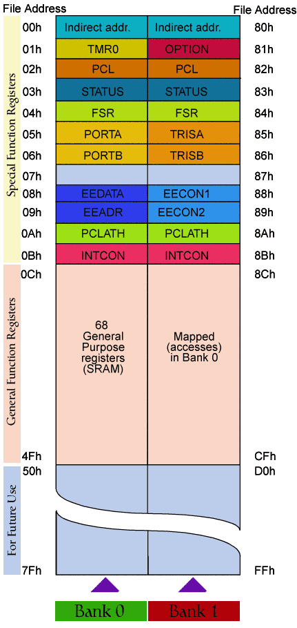
The SFRs control the operation of the device. Portions of data memory are banked. This is for both the SFR area and the GPR area. The GPR area is banked to allow greater than 116 bytes of general purpose RAM. The banked areas of the SFR are for the registers that control the peripheral functions. Banking requires the use of control bits for bank selection.These control bits are located in the STATUS Register. The figure below shows the data memory map organization. Instructions MOVWF and MOVF can move values from the W register to any location in the register file (“F”), and vice-versa.The entire data memory can be accessed either directly using the absolute address of each register file or indirectly through the File Select Register (FSR). Indirect addressing uses the present value of the RP1:RP0 bits for access into the banked areas of data memory.Data memory is partitioned into two banks which contain the general purpose registers and the special function registers. Bank 0 is selected by clearing the RP0 bit (STATUS<5>). Setting the RP0 bit selects Bank1. Each Bank extends up to 7Fh (128 bytes). The first twelve locations of each Bank are reserved for the Special Function Registers. The remainder are General Purpose Registers implemented as static RAM.
PIC16x84 Data Memory Arrangement
General Purpose Register File (GPR)Each GPR is 8 bits wide and is accessed either directly or indirectly through the FSR. The GPR addresses in bank 1 are mapped to addresses in bank 0. As an example, addressing location 0Ch or 8Ch will access the same GPR.
Special Function Registers (SFR)The Special Function Registers are used by the CPU and Peripheral functions to control the device operation. These registers are static RAM. The special function registers can be classified into two sets:
What is Bank 0 and Bank 1 and why PIC needs to use them?
One of the things that puzzled me when I started learning to use PIC microcontroller is what is memory bank0 and Bank1 and why we need to use them?. To explain this we need to look at the general format of the PIC instruction. This is explained thoroughly later in the PIC instruction set section but for this section I will use only some basics. The instruction set of the PIC16f84 consists of 14bits divided into sections : OPCode Direction of result value (d) File registers address.
General Instruction Format For Byte-oriented file register operations
The space allocated for the file registers address is 7bits wide which gives a range of addresses 0x0 - 0x7F (0000000b - 1111111b). Now to addresses locations above 0x7F we need an extra bit. This bit comes from the STATUS register (bit 5 RP0). This bit controls what is known as memory banks and is responsible for switching between two memory banks. When RP=0 Bank0 is selected and addresses range from 0x0 - 0x7F and when RP=1 Bank 1 is selected and addresses range from 0x80 - 0xFF. You can think of the Bank selection bit as the extra eighth bit in the File registers address space in the PIC instruction.
|
|||||


